File:Figure-9.jpg
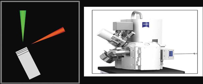
Revision as of 17:35, 15 August 2014 by Molyneux (talk | contribs) (At left, a schematic diagram of operation of an FIB-SEM system. The FIB sputters away a thin layer of the sample at a time, while the electron beam/detector system captures an image of each newly exposed surface. At right, a picture of a commercial FIB...)

Size of this preview: 800 × 334 pixels. Other resolutions: 320 × 134 pixels | 982 × 410 pixels.
Original file (982 × 410 pixels, file size: 22 KB, MIME type: image/jpeg)
At left, a schematic diagram of operation of an FIB-SEM system. The FIB sputters away a thin layer of the sample at a time, while the electron beam/detector system captures an image of each newly exposed surface. At right, a picture of a commercial FIB-SEM CrossBeam™ system, Auriga. From AAPG Memoir 102, Chapter 1, Huang et al., 2013, DOI: 10.1306/13391699M1023580.
File history
Click on a date/time to view the file as it appeared at that time.
| Date/Time | Thumbnail | Dimensions | User | Comment | |
|---|---|---|---|---|---|
| current | 17:35, 15 August 2014 | | 982 × 410 (22 KB) | Molyneux (talk | contribs) | At left, a schematic diagram of operation of an FIB-SEM system. The FIB sputters away a thin layer of the sample at a time, while the electron beam/detector system captures an image of each newly exposed surface. At right, a picture of a commercial FIB... |
You cannot overwrite this file.
File usage
The following page uses this file: